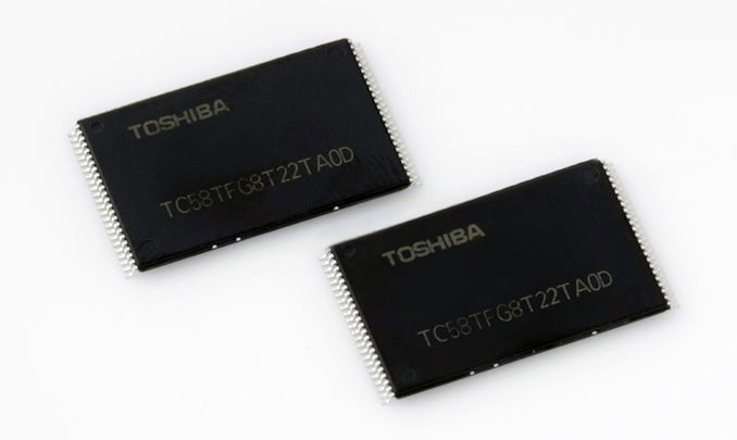
Toshiba and SanDisk Announce 48-layer 256Gbit TLC 3D NAND
by Billy Tallis on August 4, 2015 11:00 AM EST
This week Toshiba and SanDisk are announcing a new milestone in their joint development of flash memory. Back in March Toshiba announced a 48-layer 3D NAND technology that they were sampling in the form of a 128Gb MLC die. Now Toshiba and partner SanDisk have built a 256Gb TLC die on their 48-layer process. Toshiba will be sampling that chip starting in September, and SanDisk has selected it as their first 3D NAND device for mass production.
Central to this development is the outfitting of Fab 2 at their facility in Yokkaichi, Japan. The previous Fab 2 was demolished in 2014 and construction started on a replacement to be used as their first fab for 3D NAND. The new Fab 2 has now started pilot production of 3D NAND as it is being readied for mass production, scheduled to begin in 2016. Toshiba says the fab will be completed in the first half of the year and SanDisk plans to be shipping products using their 3D NAND by the end of the year.
The new 3D NAND will face experienced competition from Samsung who are currently shipping 32-layer 3D NAND in capacities up to 128Gb for both MLC and TLC configurations. Samsung has also announced its third generation V-NAND which should be starting mass production in the latter half of this year. Meanwhile, Intel and Micron have stated that their 32-layer 3D NAND will be in mass production by the fourth quarter of this year in the form of a 256Gb MLC die and a 384Gb TLC die. SK Hynix is to begin mass production of a 36-layer 128Gb MLC die during the third quarter and is working toward a 48-layer TLC that will be available in 2016.
All of the major flash manufacturers have now publicized their plans for introducing 3D NAND. Planar NAND won't be disappearing overnight or even in a year, as it takes a lot of time and money to convert a fab to a new process. But from here on out, we can expect all the most interesting news about NAND flash memory to be about 3D.
Source: Toshiba & Sandisk


28 Comments
View All Comments
MrSpadge - Tuesday, August 4, 2015 - link
This sounds very nice for "good enough" SSDs. I'd just like it paired with a controller as good as Samsungs, married to a M.2 interface. Sandisks current TLC SSDs are not very encouraging in comparison.Samus - Tuesday, August 4, 2015 - link
Wow, if my math is right that means 512GiB per chip!?extide - Tuesday, August 4, 2015 - link
No, 256Gbit = 32GBytes384Gb = 48GB
Kristian Vättö - Tuesday, August 4, 2015 - link
I think he meant per package. Currently 16 dies can be stacked in volume production, so 16x32GiB=512GiB.Impulses - Tuesday, August 4, 2015 - link
I don't even care if they keep pricing M.2 drives at a premium because I'm just gonna use a small M.2 for my boot drive, and then larger SATA drives I can RAID together for data... Going all SSD this year, goodbye spinners.I do wonder tho, going forwarded, do they intend to saddle desktop owners with mobile interfaces indefinitely or is there another SATA replacement on horizon besides Express? Does U.2 make any provision for cabled interconnects?
jjj - Tuesday, August 4, 2015 - link
Sandisk will be using 3D first in removable storage(SD cards, USB drives) and will take a while before using it in SSDs. They go TLC first and that capacity because of the market this first chip addresses. It's small enough to fit in a microSD and TLC is just fine for that market without much of a controller.KateH - Friday, August 7, 2015 - link
Unless I'm mistaken, U.2 *is* the cabled interconnect standard. Provides 4x PCIe lanes over a cable similar to SATA.KateH - Friday, August 7, 2015 - link
Looked it up- U.2 is the consumer-friendly name for SFF-8639, PCIe x4 over a mini-SAS cable (not signal-related to SAS, just reusing the commodity connector)lilmoe - Tuesday, August 4, 2015 - link
None of these will come close to the 850 EVO. Not because of the controller alone, but because of SLC cache.hojnikb - Tuesday, August 4, 2015 - link
Because sammy is the only one with "SLC" cache..