Kioxia and Western Digital Debut 218-Layer 3D NAND: 1Tb TLC with 3.2 GT/s IO Speed
by Anton Shilov on March 31, 2023 12:00 PM EST
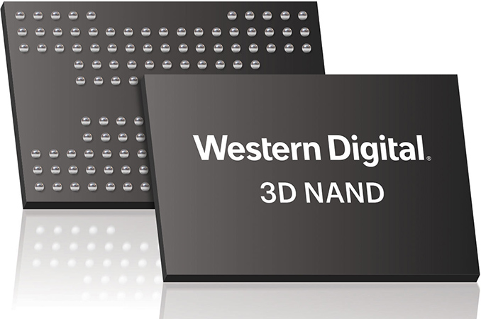
Kioxia and Western Digital formally introduced their 8th Generation BiCS 3D NAND memory with 218 active layers. The new storage device offers a 1Tb capacity in 3D TLC mode and features 3200 MT/s data transfer speed, a combination that will enable SSD makers to build high-performance, high-capacity drives. To enable such an extreme interface speed, the companies adopted an architecture akin to YMTC's Xtacking.
The 218-layer BiCS 3D NAND device jointly developed by Kioxia and Western Digital supports triple-level cell (TLC) and quad-level cell (QLC) configurations to maximize storage density and expand addressable applications. The companies said that the new device embraces their new 'lateral shrink technology to increase bit density by over 50' without elaborating. Considering that the flash memory IC increased the number of active layers by 34%, the claim about a 50% bit density increase indicates that developers also shrank lateral sizes of NAND cells to fit in more of them per layer.
Meanwhile, the 218-layer 3D NAND device features a quad-plane architecture allowing for a higher level of parallelism for programming and read times and increased performance. In addition, the 218-layer 3D TLC device also has a 3200 MT/s (which could provide a 400 MB/s peak read/write speed) input/output interface, which is the highest I/O speed announced so far. High data transfer rates will be handy for high-end client and enterprise SSDs featuring a PCIe 5.0 interface.
The key innovation of the 8th Generation BiCS 3D NAND memory is the all-new CBA (CMOS directly Bonded to Array) architecture that implicates separate production of 3D NAND cell array wafers and I/O CMOS wafers using the most optimal process technologies and then bonding them together to create a final product that offers increased bit density and fast NAND I/O speed. Meanwhile, Kioxia and Western Digital must disclose details about their CBA architecture and whether the I/O CMOS wafers carry other NAND peripheral circuitry, like page buffers, sense amplifiers, and charge pumps.
Producing memory cells and peripheral circuits separately solves several problems as it allows manufacturers to make them using the most efficient process technologies in their sections of cleanrooms. This brings further benefits as the industry adopts methods like string stacking.

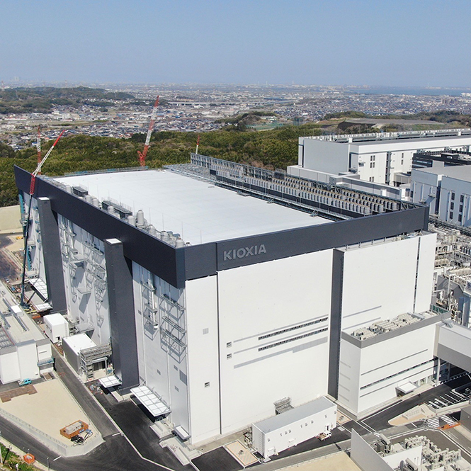
Kioxia and Western Digital Fab 7, Yokkaichi Plant, Japan
Kioxia said it had started sample shipments of 8th Generation BiCS 3D NAND memory devices to select customers. Still, there is no word when the company expects to initiate volume production of its next-generation flash memory. It is not unusual for companies to announce new types of 3D NAND quarters before they enter mass production, so it is reasonable to expect 8th Gen BICS on the market in 2024.
"Through our unique engineering partnership, we have successfully launched the eighth-generation BiCS Flash with the industry's highest bit density," said Masaki Momodomi, Chief Technology Officer at Kioxia Corporation. "I am pleased that Kioxia's sample shipments for limited customers have started. By applying CBA technology and scaling innovations, we've advanced our portfolio of 3D flash memory technologies for use in various data-centric applications, including smartphones, IoT devices, and data centers."


34 Comments
View All Comments
name99 - Friday, March 31, 2023 - link
Thanks, Anton. There was enough background explanation in this article to move it way beyond just a press release regurgitation.meacupla - Friday, March 31, 2023 - link
I don't have a good understanding of NAND chips.For reference, how does this one compare to other NAND chips?
400MB/s peak per chip doesn't sound that fast, because joining 8 of them together would only result in 3200MB/s. (Sequential or Random not specified)
This seems average when a Samsung 980 Pro 1TB will hit up to 7000MB/s sequential read/write.
Now, if that 400MB/s per chip was random read/write, then that would be very impressive.
FunBunny2 - Friday, March 31, 2023 - link
"Now, if that 400MB/s per chip was random read/write, then that would be very impressive."it's never been clear to me why sequential and random don't, by the arithmetic, work out to be (nearly) identical. we know, don't we?, that NAND/SSD data isn't stored contiguously as it is on disks, but spread all over the NAND, and importantly, re-spread during operation vis wear-leveling. so how does sequential access measure better?
Golgatha777 - Friday, March 31, 2023 - link
Might be the sustained data rate, and 3.2GB/sec would be amazing for that. Most of the sustained read/write fall off a cliff when hybrid SLC cache is exhausted. Some of my NVME drives still can't keep up with the sustained throughput of my 970 Pro SSD on large file transfers for instance. Probably the worst I've seen is a 1TB NVME I use for backup data that falls to about 100MB/sec sustained once the cache is exhausted.ballsystemlord - Friday, March 31, 2023 - link
That's quite characteristic of a QLC drive.saratoga4 - Friday, March 31, 2023 - link
>it's never been clear to me why sequential and random don't, by the arithmetic, work out to be (nearly) identical.Because of latency. There's a ~100us delay between when you start a read and when data is available. For 4KB reads at QD1 (meaning each waits for the one before to complete), that is 10,000 per second, or 40MB/s. Going faster means lower latency and NAND is optimized for density/bandwidth but not latency.
JTWrenn - Tuesday, April 4, 2023 - link
In short, the controller can't do as many small block pulls and set them up exactly right. It's not quite the same as seek time but it is really about the controller not the medium. If you look at high end enterprise controllers and ssd's the rates are much closer.JTWrenn - Tuesday, April 4, 2023 - link
Sorry to put a finer point on it....there is no such thing as a random read speed really. It's latency on the random then you start reading, then you do a find and read again. So random is usually not measure in read speed but rather the latency to find the new file/parts of a file and then it starts to read as fast as it can. Depending on the size of the file you run into efficiencies of file systems, operating systems, and controllers but generally it's two completely different things.erinadreno - Friday, March 31, 2023 - link
According to specification, ONFI uses 8 or 16bit data bus. This multiplies with 3.2GT and 4 channel can give you up to 12.8GBps bandwidth. Theoretically you can have a low end dramless 4 channel controller hitting that speed. Or more than pcie 5.0x4 can provide if you use an 8 channel controllermeacupla - Saturday, April 1, 2023 - link
okay, now that sounds fast.