Using a PCIe Slot to Install DRAM: New Samsung CXL.mem Expansion Module
by Dr. Ian Cutress on May 11, 2021 4:10 AM EST- Posted in
- Interconnect
- Samsung
- DRAM
- DDR5
- Compute Express Link
- CXL
- PCIe 5.0
- CXL.memory

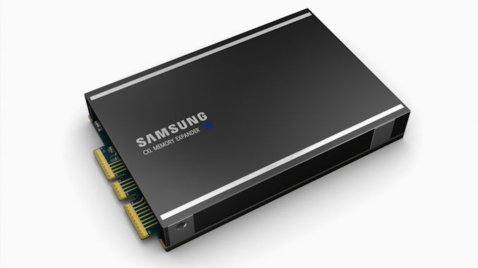
In the computing industry, we’ve lived with PCIe as a standard for a long time. It is used to add any additional features to a system: graphics, storage, USB ports, more storage, networking, add-in cards, storage, sound cards, Wi-Fi, oh did I mention storage? Well the one thing that we haven’t been able to put into a PCIe slot is DRAM – I don’t mean DRAM as a storage device, but memory that actually is added to the system as useable DRAM. Back in 2019 a new CXL standard was introduced, which uses a PCIe 5.0 link as the physical interface. Part of that standard is CXL.memory – the ability to add DRAM into a system through a CXL/PCIe slot. Today Samsung is unveiling the first DRAM module specifically designed in this way.
CXL: A Refresher
The original CXL standard started off as a research project inside Intel to create an interface that can support accelerators, IO, cache, and memory. It subsequently spun out into its own consortium, with over 50+ members, and support from key players in the industry: Intel, AMD, Arm, IBM, Broadcom, Marvell, NVIDIA, Samsung, SK Hynix, WD, and others. The latest standard is CXL 2.0, finalized in November 2020.
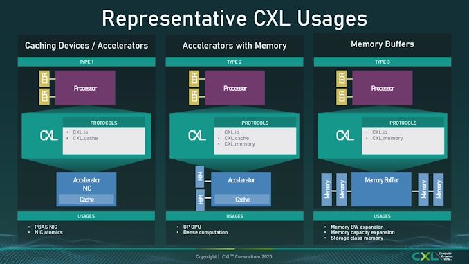
The CXL 1.1 standard covers three sets of intrinsics, known as CXL.io, CXL.memory and CXL.cache. These allow for deeper control over the connected devices, as well as an expansion as to what is possible. The CXL consortium sees three main areas for this:
The first type is a cache/accelerator, such as an offload engine or a SmartNIC (a smart network controller). With the CXL.io and CXL.cache intrinsics, this would allow the network controller to sort incoming data, analyze it, and filter what is needed directly into the main processors memory.
The second type is an accelerator with memory, and direct access to the HBM on the accelerator from the processor (as well as access to DRAM from the accelerator). The idea is a pseudo-heterogeneous compute design allowing for simpler but dense computational solvers.
The third type is perhaps the one we’re most interested in today: memory buffers. Using CXL.memory, a memory buffer can be installed over a CXL link and the attached memory can be directly pooled with the system memory. This allows for either increased memory bandwidth, or increased memory expansion, to the order of thousands of gigabytes.
CXL 2.0 also introduces CXL.security, support for persistent memory, and switching capabilities.
It should be noted that CXL is using the same electrical interface as PCIe. That means any CXL device will have what looks like a PCIe physical connector. Beyond that, CXL uses PCIe in its startup process, so currently any CXL supporting device has to also support a PCIe-to-PCIe link, making any CXL controller also a PCIe controller by default.
One of the common questions I’ve seen is what would happen if a CXL-only CPU was made? Because CXL and PCIe are intertwined, a CPU can’t be CXL-only, it would have to support PCIe connections as well. That being said, from the other direction: if we see CXL-based graphics cards for example, they would also have to at least initialize over PCIe, however full working modes might not be possible if CXL isn’t initialized.
Intel is set to introduce CXL 1.1 over PCIe 5.0 with its Sapphire Rapids processors. Microchip has announced PCIe 5.0 and CXL-based retimers for motherboard trace extensions. Samsung today is the third announcement for CXL supported devices. IBM has a similar technology called OMI (OpenCAPI Memory Interface), however that hasn’t seen wide adoption outside of IBM’s own processors.
Samsung’s CXL Memory Module
Modern processors rely on memory controllers for attached DRAM access. The top line x86 processors have eight channels of DDR4, while a number of accelerators have gone down the HBM route. One of the limiting factors in scaling up memory bandwidth is the number of controllers, which can also limit capacity, and beyond that memory needs to be validated and trained to work with a system. Most systems are not built to simply add or remove memory the same way you might do with a storage device.
Enter CXL, and the ability to add memory like a storage device. Samsung’s unveiling today is of a CXL-attached module packed to the max with DDR5. It uses a full PCIe 5.0 x16 link, allowing for a theoretical bidirectional 32 GT/s, but with multiple TB of memory behind a buffer controller. In much the same way that companies like Samsung pack NAND into a U.2-sized form factor, with sufficient cooling, Samsung does the same here but with DRAM.
The DRAM is still a volatile memory, and data is lost if power is lost. (I doubt it is hot swappable either, but weirder things have happened). Persistent memory can be used, but only with CXL 2.0. Samsung hasn't stated if their device supports CXL 2.0, but it should be at least CXL 1.1 as they state it currently is being tested with Intel's Sapphire Rapids platform.
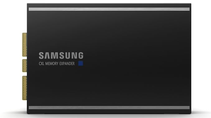
It should be noted that a modern DRAM slot is usually rated maximum for ~18W. The only modules in that power window are Intel’s Optane DCPMM, but a 256 GB DDR4 module would be in that ~10+ W range. For a 2 TB add-in CXL module like this, I suspect we are looking at around 70-80 W, and so to add that amount of DRAM through the CXL interface would likely require active cooling as well as the big heatsink that these renders suggest.
Samsung doesn’t give any details about the module they are unveiling, except that it is CXL based and has DDR5 in it. Not only that, but the ‘photos’ provided look a lot like renders, so it’s hard to state if they have an aesthetic unit available for photography, or if there’s simply a working controller in a bring-up lab somewhere that has been validated on a system. Update: Samsung has confirmed these are live shots, not renders.
As part of the announcement Samsung quoted AMD and Intel, indicating which partners they are more closely working with, and what they have today is being validated on Intel next-gen servers. Intel’s next-gen servers, Sapphire Rapids, are due to launch at the end of the year, in line with the Aurora supercomputing contract set to be initially shipped by year end.
Related Reading
- Compute eXpress Link 2.0 (CXL 2.0) Finalized: Switching, PMEM, Security
- CXL Consortium Formally Incorporated, Gets New Board Members & CXL 1.1 Specification
- CXL Specification 1.0 Released: New Industry High-Speed Interconnect From Intel
- Intel Agilex: 10nm FPGAs with PCIe 5.0, DDR5, and CXL
- Synopsys Demonstrates CXL and CCIX 1.1 over PCIe 5.0: Next-Gen In Action
- Microchip Announces PCIe 5.0 And CXL Retimers
- DDR5 Memory Specification Released: Setting the Stage for DDR5-6400 And Beyond
- Here's Some DDR5-4800: Hands-On First Look at Next Gen DRAM
- Insights into DDR5 Sub-timings and Latencies


47 Comments
View All Comments
frbeckenbauer - Tuesday, May 11, 2021 - link
So basically it's their version of IBM OMIArsenica - Tuesday, May 11, 2021 - link
Just like the article says!!Ithaqua - Wednesday, May 12, 2021 - link
So basically the 2021 version of a LIM 4 memory board.All things old are new again.
Spunjji - Tuesday, May 11, 2021 - link
Interesting stuff. I can think of a few use cases for another level of memory that slots into the memory hierarchy below system DRAM in terms of bandwidth and latency, but with additional capacity. Huge databases would be an obvious candidate.I'm sure there will also be use cases where bandwidth is so critical to performance that filling a server's PCIe allocation with lower-capacity versions of this could give a system a measurable performance boost.
deil - Tuesday, May 11, 2021 - link
read replicas god-level equipment?PCIe5, ddr5 it will take a while for us to see it in action.
koaschten - Tuesday, May 11, 2021 - link
Well, DDR5 mass production started in march 2021, but at least AMD will only adopt it with ZEN 4, from the top of my head, can't recall if Intel stated which platform will support DDR5. Eventually Alder Lake S?ET - Tuesday, May 11, 2021 - link
AMD will introduce DDR5 with Rembrandt (which is Zen3 based), probably in Q1 2022, going by their normal mobile release cycle. For desktop, who knows...And yes, Alder Lake S will support DDR5.
Yojimbo - Tuesday, May 11, 2021 - link
I'm surprised AMD are putting DDR5 in Rembrandt. Is that rumor from a good source? Cezanne is PCIe 3, for example. DDR5 is going to be more expensive than DDR4 in the beginning. So if Rembrandt will be DDR5 I assume it will only be for high-end laptop designs and it will exist alongside Cezanne in their lineup. Perhaps it will be like Alder Lake, in that it will be both DDR4 and DDR5-capable. In that case we couldn't be sure we'd actually see any DDR5 designs at launch.Santoval - Wednesday, May 12, 2021 - link
It's probably a bit more than a rumor, since it is a based on a leaked AMD roadmap. For Rembrandt they list support for LPDDR5, DDR5 and PCIe 4.0, along (click the link below). No less than 12 RDNA2 compute units are also rumored for the top Rembrandt variants (AMD needs to compete with Xe and its successors) up from 8 Vega CUs in the previous four (or is it five? I lost count for how long AMD's APUs have been stuck with Vega...) APU generations.According to the same table Rembrandt is to be released about a quarter or more before the Zen 4 based (desktop) Raphael, so the former might be released in Q4 2021, not Q1 2022.
Of course the table might well be fabricated and/or AMD's plans might change and they ditch DDR5 support for Rembrandt.
https://videocardz.com/newz/amd-ryzen-9-6900h-remb...
Santoval - Wednesday, May 12, 2021 - link
p.s. (Rembrandt is Zen 3 based, not Zen 4 based, so it may well be released a quarter or two before Raphael).