TSMC’s Version of EMIB is ‘LSI’: Currently in Pre-Qualification
by Andrei Frumusanu on August 25, 2020 2:00 PM ESTWhilst process node technologies and Moore’s Law are slowing down, manufacturers and chip designers are looking to new creative solutions to further enable device and performance scaling. Advanced packaging technologies are one such area where we’ve seen tremendous innovations over the past few years, such as the introduction of silicon interposers and integration of HBM-memory or the shift towards modularisation through chiplet designs.
Silicon interposers pose cost challenges as they are expensive and require quite a large silicon footprint, whilst chiplet designs which use conventional packaging on organic substrates are limited by I/O bandwidth and power efficiency. A solution to this problem has been the industry’s introduction of intermediary silicon dies that connect two logic chips together – but only in a limited scope, not using the same footprint as a full silicon interposer. Intel’s EMIB (Embedded Die Interconnect Bridge) has been the recently most talked about implementation of such technology.
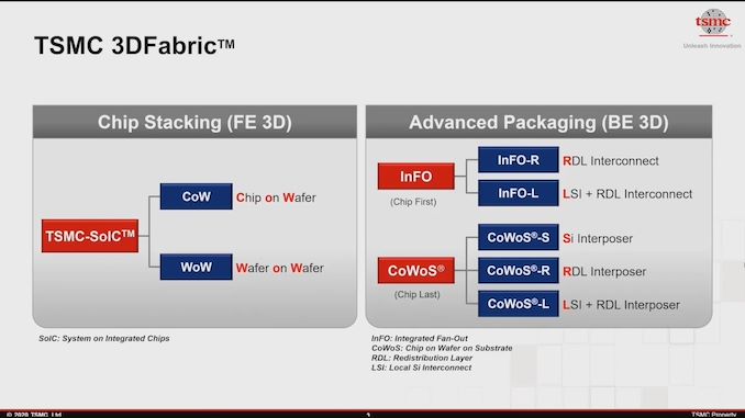
Today as TSMC’s 2020 Technology Symposium, the Taiwanese manufacturer is detailing their own variant of such a technology, called Local Si Interconnect (LSI), that will be offered for both InFO and CoWoS packaging technologies in the form of InFO-L and CoWoS-L.
The new advancements are part of what TSMC now dubs its 3DFabric packaging technology platform which offers a versatile repertoire of integration and packaging options, which include SoIC, InFO, and CoWoS.
A brief explanation for our readers unfamiliar with the terms, SoIC (System on Integrated Chip) is TSMC’s bump-less chip stacking and hybrid bonding integration technology that allows for stacking multiple chip dies together, enabling extremely high-bandwidth and low power bonding between the silicon dies. Currently, this technology has no equal in the industry.
InFO is TSMC’s fan-out packaging technology, where a silicon die from a wafer is picked out and placed on a carrier wafer, upon which the further bigger structures such as the copper RDL (Redistribution layer), and later the carrier substrate is built upon.
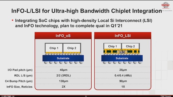
TSMC’s variant of InFO with integration of an LSI is called InFO-L or InFO-LSI, and follows a similar structure with the new addition of it integrating this new local silicon interconnect intermediary chip for communication between two chips.
TSMC’s CoWoS (Chip-on-Wafer-on-Substrate) was originally described as the company’s silicon interposer 2.5D packaging technology, which is currently still falls under the CoWoS-S specifier, but meanwhile it also covers other chip-last packaging technologies. As the description hits it at, here the base substrate, RDL are built first, and only as the last step is the target silicon chip bonded to the package.
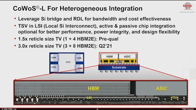
CoWoS-L is the new variant of TSMC’s chip-last packaging technology which adds in the Local Si Interconnect which is used in combination of a copper RDL to achieve higher bandwidth than just an RDL packaging implementation (CoWoS-R), and be more cost-effective than a full silicon interposer implementation (CoWoS-S).
TSMC describes the LSI as being either an active, or a passive chip, depending on chip designers needs and their cost sensitivities. The foundry expects to complete InFO-L qualification in Q1’21, and CoWoS-L is undergoing pre-qualification right now. Silicon bridge interconnect technologies such as LSI and EMIB are expected to bring high-performance chip designs at a lower cost for the designer and the consumer.
Related Reading
- TSMC Details 3nm Process Technology: Full Node Scaling for 2H22 Volume Production
- TSMC To Build 5nm Fab In Arizona, Set To Come Online In 2024
- TSMC & Broadcom Develop 1,700 mm2 CoWoS Interposer: 2X Larger Than Reticles
- TSMC Boosts CapEx by $1 Billion, Expects N5 Node to Be Major Success
- Early TSMC 5nm Test Chip Yields 80%, HVM Coming in H1 2020
- TSMC: 5nm on Track for Q2 2020 HVM, Will Ramp Faster Than 7nm
- TSMC: N7+ EUV Process Technology in High Volume, 6nm (N6) Coming Soon


17 Comments
View All Comments
jeremyshaw - Tuesday, August 25, 2020 - link
Finally, something like EMIB has been lacking from 3rd party foundries. Hopefully this can help bring the cost of HBM-type systems down.linuxgeex - Wednesday, August 26, 2020 - link
I'm not expecting it to bring costs down year on year but I am expecting it to allow significant effective layer scaling with less-than-linear cost scaling. ie we will see $10,000 chips for the datacenter with 4x as many transistors on 2x as many layers for the same cost as today's $10,000 chips.I sorely doubt we'll see an i9 / Ryzen 9 product with 8 HBM stacks in 2021, at any price point.
psychobriggsy - Wednesday, August 26, 2020 - link
Well CoWoS-S (silicon interposer) was costing $30 for sub-reticle interposers to over $100 for larger ones. Additionally, the chips to be mounted are mounted on the interposer wafer, so I guess there's some yield waste from poor assembly, poor interposers, and so on.RDLs are organic assembled interposers, and are around $3 for the same size. The LSIs will be very simple cheap silicon bridges. The assembly of the LSIs and RDLs and 'filler with TSVs' and so on looks complex of course, hence it's taken some time to come to market.
mdriftmeyer - Monday, August 31, 2020 - link
You'll be happily wrong. 2021 is Zen 4 and the first 2.5/3D process node design for them, thus there will be 8 HBM2e stacks in 2021.Spunjji - Wednesday, August 26, 2020 - link
Indeed - after a year or two I'd be hopeful of seeing an APU with console-level performance thanks to some on-package HBM acting as L4 / dedicated graphics RAM.TimSyd - Tuesday, August 25, 2020 - link
So how soon are we betting AMD will be discussing this for next gen EPYC? (Genoa etc):)
jeremyshaw - Tuesday, August 25, 2020 - link
Hopefully reducing the power penalty of Infinity Fabric?TimSyd - Tuesday, August 25, 2020 - link
Lower power & higher clocks ideally (for lower latency) :)linuxgeex - Wednesday, August 26, 2020 - link
5nm Epyc isn't on the roadmap until 2023, which is the 4 chiplet + 12 HBM roadmap from TSMC. So we might see TR and EPYC Frequency-optimised products using this in 2023. The problem is that power scale savings from 7nm to 5nm is quite small, ie <18% so that's not going to very easily increase the core budget, but it should allow a modest frequency bump, and treating the HBM like an L4 cache should help with the poor SRAM scaling.Spunjji - Wednesday, August 26, 2020 - link
Those would seem like the obvious benefits. Exciting stuff! :D