Samsung Kicks Off Mass Production of AI Chip for Baidu: 260 TOPS at 150 W
by Anton Shilov on December 18, 2019 11:00 AM EST- Posted in
- AI
- Samsung
- SoCs
- 14nm
- Machine Learning
- Baidu
- Samsung Foundry
- Kunlun

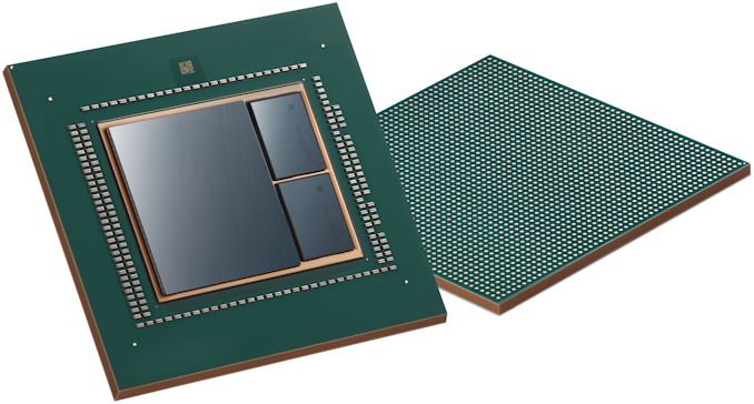
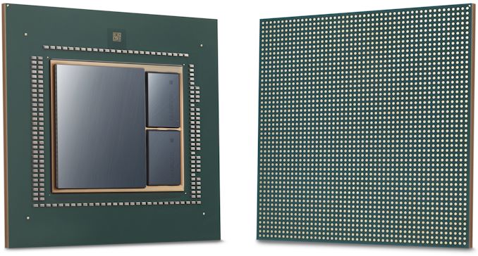
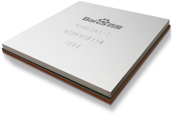
Samsung Foundry and Baidu this week said that the companies were about to start mass production of an AI accelerator chip early in 2020. Baidu’s Kunlun chip is to be made using Samsung’s proven 14 nm process technology, and make use of the company’s Interposer-Cube 2.5D packaging structure.
The Baidu Kunlun AI accelerator is based on the company’s XPU neural processor architecture that uses thousands of small cores that can be used for a wide variety of applications in the cloud and on the edge of networks. The chip provides up to 260 Trillion operations per second (TOPS) at 150 Watts, and features 512 GB/s memory bandwidth using two HBM2 memory packages. It is noteworthy that when the SoC was introduced back in mid-2018, its TDP was described at falling in at 100 Watts, so it seems the final product missed the initial power consumption goals.
According to Baidu, its Kunlun chip is three times faster in the ERNIE (Enhanced Language Representation with Informative Entities) inference application than a traditional GPU or FPGA. In addition, it can be used for autonomous driving (assuming that its 150 W TDP can be mitigated), speech recognition, image processing, and deep learning.
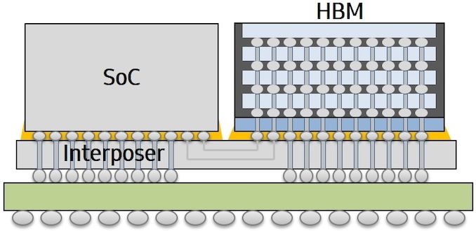
The Kunlun is one of the first AI accelerator that uses I-Cube packaging and is made by Samsung Foundry. The 2.5D packaging uses an interposer and is expected to enable Samsung to build other accelerator chips that require high memory bandwidth, and therefore make use of their HBM2 memory offerings. In addition, the company is developing other advanced packaging solutions, including redistribution layers (RDL), as well as denser HBM packages.
Ryan Lee, vice president of foundry marketing at Samsung Electronics, said the following:
“Baidu Kunlun is an important milestone for Samsung Foundry as we are expanding our business area beyond mobile to datacenter applications by developing and mass-producing AI chips. Samsung will provide comprehensive foundry solutions from design support to cutting-edge manufacturing technologies, such as 5LPE, 4LPE, as well as 2.5D packaging.”
Related Reading:
- Intel's Xeon Cascade Lake vs. NVIDIA Turing: An Analysis in AI
- AI On The Edge: New Flex Logix X1 Inference AI Chip For Fanless Designs
- The AI Race Expands: Qualcomm Reveals “Cloud AI 100” Family of Datacenter AI Inference Accelerators for 2020
- Hot Chips 31 Live Blogs: Xilinx Versal AI Engine
- Cambricon, Makers of Huawei's Kirin NPU IP, Build A Big AI Chip and PCIe Card
Source: Samsung


9 Comments
View All Comments
s.yu - Wednesday, December 18, 2019 - link
Interesting new customer.Drumsticks - Wednesday, December 18, 2019 - link
I wish there was more information on this. 260 TOPs at what size? Presumably INT8, since its referenced as an inference chip, but INT4 isn't necessarily impossible. 260 TOPs at INT8 is still pretty impressive, but it's not mind bending if it's just INT4.nandnandnand - Wednesday, December 18, 2019 - link
This is 260 TOPS at 150 Watts on a 14nm node.Compared to 200 TOPS (INT8) likely at 65-70 Watts, on a 5nm or 7nm node for the Nvidia DRIVE AGX Orin.
I'm going to assume INT8 but who knows.
Alistair - Wednesday, December 18, 2019 - link
If it is INT8 isn't it faster than the chip that nVidia announced to come out 3 years from now?nandnandnand - Wednesday, December 18, 2019 - link
Sure, but it uses more energy.1.73 TOPS/Watt vs. at least 2.86 TOPS/Watt (according to AnandTech's guess for TDP)
Santoval - Wednesday, December 18, 2019 - link
It also appears to be a strictly AI processor, with no general purpose cores, a GPU or anything else but tensor cores (and, of course, the memory controllers to speak with the HBM2 dies). That means that an additional general purpose CPU or SoC is required to control and program this. An extra CPU means higher cost and an even higher power draw.Arnulf - Saturday, December 21, 2019 - link
Sure, but it has HBM2 baked in and is actually being produced as we speak, on an older (less efficient) process.Santoval - Wednesday, December 18, 2019 - link
Almost certainly INT8.Fataliity - Thursday, December 19, 2019 - link
It is noteworthy that when the SoC was introduced back in mid-2018, its TDP was described at falling in at 100 Watts-- For some reason, most of these companies don't include the power of HBM and other stuff when calculating TDP. Only the Compute Chip itself..