The NVIDIA Turing GPU Architecture Deep Dive: Prelude to GeForce RTX
by Nate Oh on September 14, 2018 12:30 PM ESTFeeding the Beast (2018): GDDR6 & Memory Compression
Memory bandwidth has always been a challenge for video cards, and that challenge only continues to get harder. Thanks to the mechanics of Moore’s Law, GPU transistor counts – and therefore the quantities of various cores – is growing at a rapid pace. Meanwhile DRAM, whose bandwidth is not subject to the same laws, has grown at a much smaller pace.
The net result is that with nearly every generation, the amount of memory bandwidth available per FLOP, per texture lookup, and per pixel blend has continued to drop. So to keep GPU performance scaling – to feed the great graphical beast – GPU manufacturers and the memory industry as a whole have to look for new ways to boost memory bandwidth for future memory technologies while reducing the amount of memory bandwidth they’re using right now. Neither is easy, and both are areas where NVIDIA has been executing well on over most of the past decade, making it an architectural strength for the company.
| NVIDIA Memory Bandwidth per FLOP (In Bits) | ||||||
| GPU | Bandwidth/FLOP | Total CUDA FLOPs | Total Bandwidth | |||
| RTX 2080 | 0.36 bits | 10.06 TFLOPs | 448GB/sec | |||
| GTX 1080 | 0.29 bits | 8.87 TFLOPs | 320GB/sec | |||
| GTX 980 | 0.36 bits | 4.98 TFLOPs | 224GB/sec | |||
| GTX 680 | 0.47 bits | 3.25 TFLOPs | 192GB/sec | |||
| GTX 580 | 0.97 bits | 1.58 TFLOPs | 192GB/sec | |||
Turing, in turn, is a bit of an interesting swerve in this pattern thanks to its heavy focus on ray tracing and neural network inferencing. If we're looking at memory bandwidth merely per CUDA core FLOP, then bandwidth per FLOP has actually gone up, since RTX 2080 doesn't deliver a significant increase in (on-paper) CUDA core throughput relative to GTX 1080. However RTX 2080 also now has to feed ray tracing cores and tensor cores, both of which are very bandwidth hungry on their own. So while in pure, FP32 core compute scenarios the situation has improved a bit, once the entire GPU is put to work, the amount of contention for memory bandwidth is still higher than ever.
In terms of memory technologies, the 16nm/14nm generation of GPUs saw an interesting and atypical divergence in the memory space. GDDR5, which has been with us for a decade now, has been ripe for replacement. The JEDEC, the industry standardization body responsible for setting common memory standards, initially approached this in two directions. The first route was more traditional, developing a successor technology to GDDR5, which became GDDR5X. Meanwhile the more radical approach was ultra-wide I/O technologies, which became the High Bandwidth Memory (HBM) standards.
NVIDIA for their part embraced both, but at different levels. HBM is very powerful, but the realities of wide I/O make it harder to manufacture and more costly to put on a product, thanks to the need for a silicon interposer. As a result, HBM (and specifically, HBM2) has only ever been used on NVIDIA’s flagship compute GPUs, the GP100 and GV100. For everything else, NVIDIA turned to GDDR5X. And this is where things get a bit odd.
GDDR5X is a JEDEC standard like GDDR5 before it, but it simply never saw the same kind of adoption that GDDR5 did. This goes both for memory vendors and GPU vendors. Only Micron ever produced the memory, and only NVIDIA ever used it. So the fastest Pascal cards – GTX 1080, GTX 1080 Ti, & Titan Xp – are outliers in that they’re the only (consumer) cards using this memory technology. GDDR5X was an important piece of the Pascal puzzle as it allowed NVIDIA to better feed their fastest cards, but in time it has essentially became a dead-end branch of GDDR memory technology as it never saw the kind of adoption required to reach critical mass.
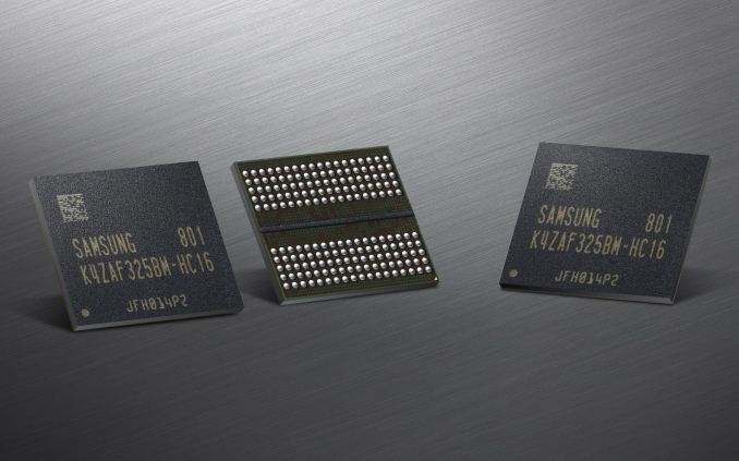
So where did GDDR branch to instead? This brings us to GDDR6, the latest and greatest in GDDR memory technology. And unlike GDDR5X before it, GDDR6 has the full backing of the Big 3 memory manufacturers – Samsung, SK Hynix, and Micron – so the memory industry as a whole has a much larger stake in the technology. For NVIDIA’s products, this is evident right off the bat: NVIDIA is using Samsung’s 16Gb capacity GDDR6 modules for their Quadro cards, and meanwhile they’re tapping Micron’s 8Gb modules for the new GeForce RTX cards.
The performance impact of GDDR6, in turn, depends in part on what we’re comparing it to. Relative to GDDR5X, GDDR6 is not quite as big of a step up as some past memory generations, as many of GDDR6’s innovations were already baked into GDDR5X. GDDR5 officially topped out at 8Gbps per pin (with NV working with partners to do 9Gbps overclocked SKUs), while NVIDIA shipped GDDR5X cards clocked as high as 11.4Gbps. GDDR6, in turn, is going to be starting at 14Gbps in graphics cards, with future generations of the technology set to reach 16Gbps and higher. So for the likes of NVIDIA’s x70 cards, the switch from GDDR5 to GDDR6 is going to be one of those massive once-in-a-generation bandwidth jumps. However for NVIDIA’s x80 cards, the upgrade from GDDR5X to GDDR6 is going to give those products a healthy increase in memory bandwidth, it just won’t be a huge jump.
Diving a bit deeper here, there are really two core changes coming from GDDR5 that enable GDDR6’s big bandwidth boost. The first is the implementation of Quad Data Rate (QDR) signaling on the memory bus. Whereas GDDR5’s memory bus would transfer data twice per write clock (WCK) via DDR, GDDR6 (& 5X) extends this to four transfers per clock. All other things held equal, this allows GDDR6 to transfer twice as much data per clock as GDDR5.
The challenge in doing this, of course, is that the more you pump a memory bus, the tighter the signal integrity requirements. So while it’s simple to say “let’s just double the memory bus bandwidth”, doing it is another matter. In practice a lot of work goes into the GPU memory controller, the memory itself, and the PCB to handle these transmission speeds.
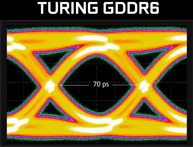
Every time NVIDIA launches support for a new memory technology, they like to roll out a new “eye diagram” signal analysis graph. And while at a high level these things don’t tell us anything we don’t already know – that NVIDIA has the technology working, and that, if it wasn’t, they wouldn’t publish these – they’re none the less neat to see. In this case we’re looking at a fairly clean eye diagram, illustrating the very tight 70ps transitions between data transfers. NVIDIA says that they were able to reduce signal crosstalk by 40% here, which is one of the key signal integrity changes required to make GDDR6’s high speed signaling possible.
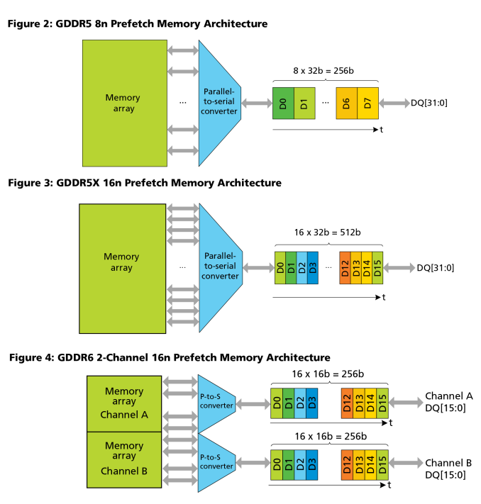
Moving on, the second big change for GDDR6 is that how data is read out of the DRAM cells themselves has changed. For many generations the solution has been to just read and write in larger strides – the prefetch value – with GDDR5 taking this to 8n and GDDR5X taking it to 16n. However the resulting access granularities of 32 bytes and 64 bytes respectively were on the path of becoming increasingly suboptimal for small memory operations. As a result, GDDR6 does a larger prefetch and yet it does not.
Whereas both GDDR5 and GDDR5X used a single 32-bit channel per chip, GDDR6 instead uses a pair of 16-bit channels. This means that in a single memory core clock cycle (ed: not to be confused with the memory bus), 32 bytes will be fetched from each channel for a total of 64 bytes. This means that each GDDR6 memory chip can fetch twice as much data per clock as a GDDR5 chip, but it doesn’t have to be one contiguous chunk of memory. In essence, each GDDR6 memory chip can function like two chips.
For graphics this doesn’t have much of an impact since GPUs already read and write to RAM in massive sequential parallelism. However it’s a more meaningful change for other markets. In this case the smaller memory channels will help with random access performance, especially compared to GDDR5X and its massive 64 byte access granularity.
Moving on, GDDR6 also implements some changes to further reduce power consumption – or perhaps it’s better to say that these keep power consumption from continuing to grow. The standard operating voltage for the memory technology is 1.35v; this is identical to GDDR5X’s 1.35v voltage, but down from 1.5v for standard GDDR5.
The actual power savings are a bit hard to quantify here, as NVIDIA has rolled that data into all of their memory controller optimizations. But at least publicly, what they are saying is that in conjunction with “extensive” clock gating, they’ve been able to improve power efficiency by 20% over Pascal and GDDR5X, and undoubtedly by more versus Pascal paired with GDDR5. That said, these numbers should be taken with a small grain of salt, as these numbers appear to be averages rather than peaks. NVIDIA’s clock gating enhancements are primarily about reducing power consumption when GDDR6 is not running at full utilization, so peak power may be another story.
| GPU Memory Math: GDDR6 vs. HBM2 vs. GDDR5X | ||||||||
| NVIDIA GeForce RTX 2080 Ti (GDDR6) |
NVIDIA GeForce RTX 2080 (GDDR6) |
NVIDIA Titan V (HBM2) |
NVIDIA Titan Xp |
NVIDIA GeForce GTX 1080 Ti | NVIDIA GeForce GTX 1080 | |||
| Total Capacity | 11 GB | 8 GB | 12 GB | 12 GB | 11 GB | 8 GB | ||
| B/W Per Pin | 14 Gb/s | 1.7 Gb/s | 11.4 Gbps | 11 Gbps | ||||
| Chip capacity | 1 GB (8 Gb) | 4 GB (32 Gb) | 1 GB (8 Gb) | |||||
| No. Chips/KGSDs | 11 | 8 | 3 | 12 | 11 | 8 | ||
| B/W Per Chip/Stack | 56 GB/s | 217.6 GB/s | 45.6 GB/s | 44 GB/s | ||||
| Bus Width | 352-bit | 256-bit | 3092-bit | 384-bit | 352-bit | 256-bit | ||
| Total B/W | 616 GB/s | 448GB/s | 652.8 GB/s | 547.7 GB/s | 484 GB/s | 352 GB/s | ||
| DRAM Voltage | 1.35 V | 1.2 V (?) | 1.35 V | |||||
All told then, NVIDIA will be the first GPU manufacturer to roll out GDDR6 support. And with the GTX 2070 on-up having all been announced already, it’s already going to be a wider roll-out than what we saw for GDDR5X. And to put things in numbers, relative to the GTX 10 series, the RTX 2080 Ti will get 27% more memory bandwidth, the RTX 2080 40% more bandwidth, and the RTX 2070 a whopping 75% more memory bandwidth than its predecessor.
However as this is a brand-new memory technology, I’m not sure whether we’re going to see it on the obligatory 2060 & 2050 cards. In transition periods, these tiers have been known to use older memory for cost and supply reasons – so we’ll have to see what happens.
Finally, just as GDDR6 is already seeing greater adoption on the memory manufacturer side, I’m expecting the same on the GPU side. AMD hasn’t announced their plans thus far, but I will be greatly surprised if we see them skip out on GDDR6 like they did GDDR5X.
Turing: Memory Compression Iterated
As I stated at the start of this section, the key to improving GPUs is to tackle the problem from two directions: increase the available memory bandwidth, and then decrease how much of it you use. For the latter, NVIDIA has employed a number of tricks over the years. Perhaps the most potent of which (that they’re willing to talk about, at least) being their memory compression technology.
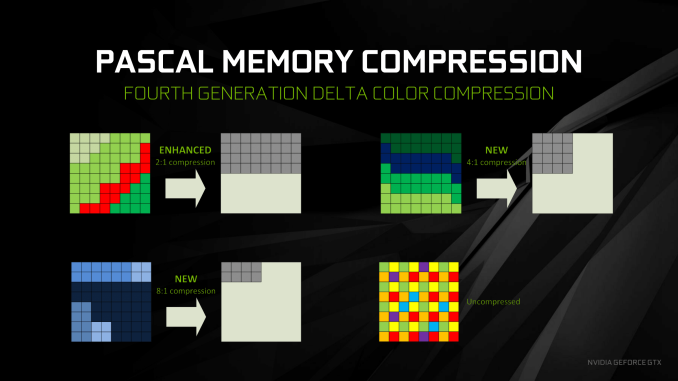
The cornerstone of memory compression is what is called data color compression. DCC is a per-buffer/per-frame compression method that breaks down a frame into tiles, and then looks at the differences between neighboring pixels – their deltas. By utilizing a large pattern library, NVIDIA is able to try different patterns to describe these deltas in as few pixels as possible, ultimately conserving bandwidth throughout the GPU, not only reducing DRAM bandwidth needs, but also L2 bandwidth needs and texture unit bandwidth needs (in the case of reading back a compressed render target).
With Pascal, NVIDIA rolled out their 4th generation technology, and now with Turing we’re at the 5th generation. Unfortunately, details on what the 5th generation entails are very slim; NVIDIA just isn’t talking about the technology much. The nature of DCC is such that it’s meant to be expandable: more silicon can be devoted to allowing more patterns to be checked at once. So it’s practically guaranteed that NVIDIA has once again expanded their library of patterns. However what those expanded patterns are, we don’t know.
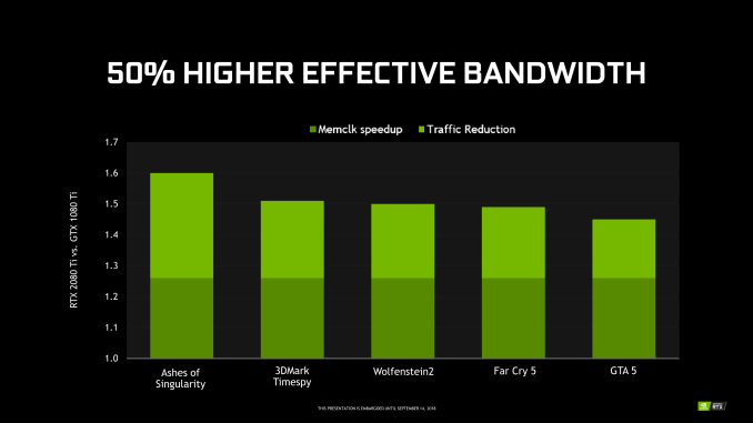
However of the limited information NVIDIA has released, they’ve offered some effective memory bandwidth graphs, with the results broken down into how much of that gain came from actual memory bandwidth increases, and then how much of that came from efficiency increases. In NVIDIA’s examples the effective increase in bandwidth varies by game; as this is the RTX 2080 Ti, GDDR6 provides a constant 27% of the improvement, while the rest of the improvement is variable based on how useful NVIDIA’s memory compression updates are to the given game.
Overall, NVIDIA is seeing anywhere between a 45% increase in effective memory bandwidth for Grand Theft Auto V, up to a 60% increase for Ashes of the Singularity. Which, if we subtract out the base 27% memory clock increase, means that the efficiency increases are between 18% and 33%.
More broadly speaking, NVIDIA is claiming a 50% increase in effective memory bandwidth for the RTX 2080 Ti versus the GTX 1080 Ti. Which again subtracting the base 27% memory bandwidth increase from GDDR6, leaves us with an average efficiency improvement of 23%.
Relative to Pascal then, this is a smaller increase in effective memory bandwidth, but a slightly larger increase in compression efficiency. For Pascal – and specifically, GTX 1080 – NVIDIA claimed a 70% effective memory bandwidth increase, of which 20% was compression improvements.
So while NVIDIA isn’t gaining as much effective memory bandwidth this time around due to the smaller step up from GDDR5X to GDDR6, their compression gains have actually improved a bit between generations. Which is actually a bit surprising, as I would have otherwise expected diminishing returns in the gains from memory compression. After all, NVIDIA started with the most commonly seen pixel patterns, and each generation of DCC would be adding less common patterns.




111 Comments
View All Comments
xXx][Zenith - Friday, September 14, 2018 - link
Nice write-up! With 25% of the chip area dedicated to Tensor Cores and other 25% to RT Cores NVIDIA is betting big on DLSS and RTX for gaming usecases. With all the architectural improvements, better memory compression ... AMD is out of the game, quite frankly.Btw, for the fans of GigaRays/Sec, aka CEO metric, here is a Optix-RTX benchmark for Volta, Pascal and Maxwell GPUs: https://www.youtube.com/watch?v=ULtXYzjGogg
OptiX 5.1 API will work with Turing GPUs but will not take advantage of the new RT Cores, so older-gen NV GPUs can be directly compared to Turing. Application devs need to rebuild with Optix 5.2 to get access to HW accelarated ray tracing. Imho, RTX cards will have nice speedup with Turing RT Cores using GPU renderers (Octane, VRay, ...) but the available RAM will limit the scene complexity big time.
blode - Friday, September 14, 2018 - link
hate when i lose a game before my opponent arriveseddman - Friday, September 14, 2018 - link
As far as I can tell, GigaRays/Sec is not an nvidia made term. It's been used before by others too, like imagination tech.The nvidia made up term is RTX-ops.
xXx][Zenith - Friday, September 14, 2018 - link
Ray tracing metric without scene complexity, viewport placement is just smoke and mirrors ...From whitepaper: "Turing ray tracing performance with RT Cores is significantly faster than ray tracing in Pascal GPUs. Turing can deliver far more Giga Rays/Sec than Pascal on different workloads, as shown in Figure 19. Pascal is spending approximately 1.1 Giga Rays/Sec, or 10 TFLOPS / Giga Ray to do ray tracing in software, whereas Turing can do 10+ Giga Rays/Sec using RT Cores, and run ray tracing 10 times faster."
eddman - Saturday, September 15, 2018 - link
I don't know the technical details of ray tracing, but how is that nvidia statement related to scene complexity, etc?From my understanding of that statement, they are simply saying that turing is able to deliver far more rays/sec than pascal, because it is basically hardware-accelerating the operations through RT cores but pascal has to do all those operations in software through regular shader cores.
niva - Wednesday, September 19, 2018 - link
If you hold scene complexity constant (take the same environment/angle) and run a ray tracing experiment, the new hardware will be that much faster at cranking out frames. At least that's how I'm interpreting the article and the statement above, I'm not really sure if that's accurate though...Yojimbo - Saturday, September 15, 2018 - link
When did Imgtec use gigarays? As far as I remember they didn't have hardware capable of a gigaray. They measured in hundreds of millions of rays per second, and I don't remember them using the term "megaray", either. Just something along the lines of "200 million rays/sec".eddman - Saturday, September 15, 2018 - link
Why fixate on the "giga" part? I obviously meant rays/sec; forgot top remove the giga part after copy/paste. A measuring method doesn't change with quantity.Yojimbo - Saturday, September 15, 2018 - link
Because the prefix is the whole point. The point is the terminology, not the measuring method. Rays per second is pretty obvious and has probably been around since the 70s. The "CEO metric" the OP was talking about was specifically about "gigarays per second". Jensen Huang said it during his SIGGRAPH presentation. Something like "Here's something you probably haven't heard before. Gigarays. We have gigarays."eddman - Saturday, September 15, 2018 - link
What are you on about? He meant "giga" as in "billion". It's so simple. He said it that way to make it sound impressive.