High-NA
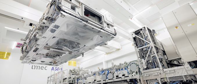
Imec and ASML have announced that the two companies have printed the first logic and DRAM patterns using ASML's experimental Twinscan EXE:5000 EUV lithography tool, the industry's first High-NA EUV scanner. The lithography system achieved resolution that is good enough for 1.4nm-class process technology with just one exposure, which confirms the capabilities of the system and that development of the High-NA ecosystem remains on-track for use in commercial chip production later this decade. "The results confirm the long-predicted resolution capability of High NA EUV lithography, targeting sub 20nm pitch metal layers in one single exposure," said Luc Van den hove, president and CEO of imec. "High NA EUV will therefore be highly instrumental to continue the dimensional scaling of logic and memory technologies, one of...
ASML Patterns First Wafer Using High-NA EUV Tool, Ships Second High-NA Scanner
This week ASML is making two very important announcements related to their progress with high numerical aperature extreme ultraviolet lithography (High-NA EUV). First up, the company's High-NA EUV prototype...
13 by Anton Shilov on 4/18/2024IFS Reborn as Intel Foundry: Expanded Foundry Business Adds 14A Process To Roadmap
5 nodes in 4 years. This is what Intel CEO Pat Gelsinger promised Intel’s customers, investors, and the world at large back in 2021, when he laid out Intel’s...
29 by Ryan Smith on 2/21/2024ASML to Ship Multiple High-NA Tools in 2025, Expands Production Capacities
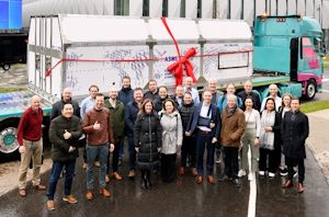
ASML began to ship its first High-NA lithography tool to Intel late last year ,and the machine will be fully assembled in Oregon in the coming months. Shipping only...
8 by Anton Shilov on 2/14/2024ASML's First High-NA EUV Litho Scanner Arrives At Intel [UPDATED]
Update 1/5/2024: Intel Oregon announced on Thursday that it has received its shipment of ASML's first-generation Twinscan EXE:5000 High-NA EUV lithography scanner. The two companies will start assembly process...
28 by Anton Shilov on 1/5/2024Intel High-NA Lithography Update: Dev Work On Intel 18A, Production On Future Node
As part of Intel’s suite of hardware announcements at this year’s Intel Innovation 2023 conference, the company offered a brief update on their plans for High-NA EUV machines, which...
24 by Ryan Smith on 9/20/2023ASML to Deliver First High-NA EUV Tool This Year
In a promising sign for the development of the next generation of EUV lithography machines, ASML has revealed that the company is set to deliver the industry's first High-NA...
7 by Anton Shilov on 9/6/2023Samsung Seeks to Make South Korea No. 1 Chipmaker with $230B Investment Over 20 Years
Samsung on Wednesday unveiled their plan to invest $230 billion over the next 20 years in a new semiconductor production mega cluster in South Korea. The country's government believes...
22 by Anton Shilov on 3/15/2023ASML High-NA Development Update: Coming to Fabs in 2024 - 2025
It took the semiconductor industry over a decade to prep everything needed for production of chips using extreme ultraviolet (EUV) lithography. It looks like it is going to take...
8 by Anton Shilov on 5/26/2022Intel Opens D1X-Mod3 Fab Expansion; Moves Up Intel 18A Manufacturing to H2’2024
Intel for the last few years has been undergoing a major period of manufacturing expansion for the company. While the more recent announcements of new facilities in Ohio and...
91 by Ryan Smith on 4/11/2022EUV Wafers Processed and TwinScan Machine Uptime: A Quick Look
One of the interesting elements that came out of some of our discussions at the IEDM conference this year revolve around the present deployment of EUV. Currently only one...
29 by Dr. Ian Cutress on 12/11/2019

