Intel 3rd Gen Xeon Scalable (Ice Lake SP) Review: Generationally Big, Competitively Small
by Andrei Frumusanu on April 6, 2021 11:00 AM EST- Posted in
- Servers
- CPUs
- Intel
- Xeon
- Enterprise
- Xeon Scalable
- Ice Lake-SP
Test Bed and Setup - Compiler Options
For the rest of our performance testing, we’re disclosing the details of the various test setups:
Intel - Dual Xeon Platinum 8380
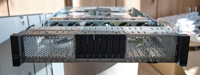
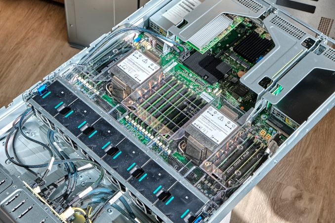
For our new Ice Lake test system based on the Whiskey Lake platform, we’re using Intel’s SDP (Software Development Platform 2SW3SIL4Q, featuring a 2-socket Intel server board (Coyote Pass).
The system is an airflow optimised 2U rack unit with otherwise little fanfare.
Our review setup solely includes the new Intel Xeon 8380 with 40 cores, 2.3GHz base clock, 3.0GHz all-core boost, and 3.4GHz peak single core boost. That’s unusual about this part as noted in the intro, it’s running at a default 205W TDP which is above what we’ve seen from previous generation non-specialised Intel SKUs.
| CPU | 2x Intel Xeon Platinum 8380 (2.3-3.4 GHz, 40c, 60MB L3, 270W) |
| RAM | 512 GB (16x32 GB) SK Hynix DDR4-3200 |
| Internal Disks | Intel SSD P5510 7.68TB |
| Motherboard | Intel Coyote Pass (Server System S2W3SIL4Q) |
| PSU | 2x Platinum 2100W |
The system came with several SSDs including Optane SSD P5800X’s, however we ran our test suite on the P5510 – not that we’re I/O affected in our current benchmarks anyhow.
As per Intel guidance, we’re using the latest BIOS available with the 270 release microcode update.
Intel - Dual Xeon Platinum 8280
For the older Cascade Lake Intel system we’re also using a test-bench setup with the same SSD and OS image as on the EPYC 7742 system.
Because the Xeons only have 6-channel memory, their maximum capacity is limited to 384GB of the same Micron memory, running at a default 2933MHz to remain in-spec with the processor’s capabilities.
| CPU | 2x Intel Xeon Platinum 8280 (2.7-4.0 GHz, 28c, 38.5MB L3, 205W) |
| RAM | 384 GB (12x32 GB) Micron DDR4-3200 (Running at 2933MHz) |
| Internal Disks | Crucial MX300 1TB |
| Motherboard | ASRock EP2C621D12 WS |
| PSU | EVGA 1600 T2 (1600W) |
The Xeon system was similarly run on BIOS defaults on an ASRock EP2C621D12 WS with the latest firmware available.
AMD - Dual EPYC 7763 / 7713 / 75F3 / 7662
In terms of testing the new EPYC 7003 series CPUs, unfortunately due to our malfunctioning Daytona server, we weren’t able to get first-hand experience with the hardware. AMD graciously gave us remote access to one of their server clusters – we had full controls of the system in terms of BMC as well as BIOS settings.
| CPU | 2x AMD EPYC 7763 (2.45-3.500 GHz, 64c, 256 MB L3, 280W) / 2x AMD EPYC 7713 (2.00-3.365 GHz, 64c, 256 MB L3, 225W) / 2x AMD EPYC 75F3 (3.20-4.000 GHz, 32c, 256 MB L3, 280W) / 2x AMD EPYC 7662 (2.00-3.300 GHz, 64c, 256 MB L3, 225W) |
| RAM | 512 GB (16x32 GB) Micron DDR4-3200 |
| Internal Disks | Varying |
| Motherboard | Daytona reference board: S5BQ |
| PSU | PWS-1200 |
Software wise, we ran Ubuntu 20.10 images with the latest release 5.11 Linux kernel. Performance settings both on the OS as well on the BIOS were left to default settings, including such things as a regular Schedutil based frequency governor and the CPUs running performance determinism mode at their respective default TDPs unless otherwise indicated.
AMD - Dual EPYC 7742
Our local AMD EPYC 7742 system, due to the aforementioned issues with the Daytona hardware, is running on a SuperMicro H11DSI Rev 2.0.
| CPU | 2x AMD EPYC 7742 (2.25-3.4 GHz, 64c, 256 MB L3, 225W) |
| RAM | 512 GB (16x32 GB) Micron DDR4-3200 |
| Internal Disks | Crucial MX300 1TB |
| Motherboard | SuperMicro H11DSI0 |
| PSU | EVGA 1600 T2 (1600W) |
As an operating system we’re using Ubuntu 20.10 with no further optimisations. In terms of BIOS settings we’re using complete defaults, including retaining the default 225W TDP of the EPYC 7742’s, as well as leaving further CPU configurables to auto, except of NPS settings where it’s we explicitly state the configuration in the results.
The system has all relevant security mitigations activated against speculative store bypass and Spectre variants.
Ampere "Mount Jade" - Dual Altra Q80-33
The Ampere Altra system we’re using the provided Mount Jade server as configured by Ampere. The system features 2 Altra Q80-33 processors within the Mount Jade DVT motherboard from Ampere.
In terms of memory, we’re using the bundled 16 DIMMs of 32GB of Samsung DDR4-3200 for a total of 512GB, 256GB per socket.
| CPU | 2x Ampere Altra Q80-33 (3.3 GHz, 80c, 32 MB L3, 250W) |
| RAM | 512 GB (16x32 GB) Samsung DDR4-3200 |
| Internal Disks | Samsung MZ-QLB960NE 960GB Samsung MZ-1LB960NE 960GB |
| Motherboard | Mount Jade DVT Reference Motherboard |
| PSU | 2000W (94%) |
The system came preinstalled with CentOS 8 and we continued usage of that OS. It’s to be noted that the server is naturally Arm SBSA compatible and thus you can run any kind of Linux distribution on it.
The only other note to make of the system is that the OS is running with 64KB pages rather than the usual 4KB pages – this either can be seen as a testing discrepancy or an advantage on the part of the Arm system given that the next page size step for x86 systems is 2MB – which isn’t feasible for general use-case testing and something deployments would have to decide to explicitly enable.
The system has all relevant security mitigations activated, including SSBS (Speculative Store Bypass Safe) against Spectre variants.
The system has all relevant security mitigations activated against the various vulnerabilities.
Compiler Setup
For compiled tests, we’re using the release version of GCC 10.2. The toolchain was compiled from scratch on both the x86 systems as well as the Altra system. We’re using shared binaries with the system’s libc libraries.


169 Comments
View All Comments
deil - Tuesday, April 6, 2021 - link
that's a lot of upgrade for intelGomez Addams - Tuesday, April 6, 2021 - link
That is a curious-looking wafer. I thought it was fake at first but then I noticed the alignment notch. Actually, I'm still not convinced it's real because I have seen lots and lots of wafers in various stages of production and I have never seen one where partial chips go all the way out to the edges. It's a waste of time to deal with those in the steppers so no one does that.JCB994 - Tuesday, April 6, 2021 - link
Periphery defects? I used to deal with those...buildup of material that would breakdown during wet processing and stream particles all over the wafer. Running partials as far out as possible helped. Nowadays...do they still use big wet benches? I have been out awhile...Gomez Addams - Tuesday, April 6, 2021 - link
Yes, they do. That's one of the systems I spent lots of time working on. Those don't look defects to me. They are just a continuation of the chip pattern.FullmetalTitan - Saturday, April 24, 2021 - link
Still the most chemical efficient tools for some etch processes. It is odd to see die prints out to the edge all around, usually at least the 'corners' are inked out/not patterned by the time it hits copper layers because printing features out that far can increase the chances of film delamination, which just leads to more defectivity. I suppose on DUV tools the extra few seconds to run those shots isn't THAT bad on non-immersion layers, but it adds up over timeArsenica - Tuesday, April 6, 2021 - link
It isn´t real if it doesn´t have DrIan bite marks./jk
ilt24 - Tuesday, April 6, 2021 - link
@Gomez AddamsI spent my entire career working in the semiconductor industry, although in IT, and I have seen many wafers from 4" to 12" and printing partial die off the edge of the wafer is quite common.
check out the pictures in these article:
https://www.anandtech.com/show/15380/i-ran-off-wit...
https://www.anandtech.com/show/9723/amd-to-spinoff...
Kamen Rider Blade - Tuesday, April 6, 2021 - link
So when are we going to hit 450 mm / 18" waffers?Are we ever going to get Hexagonal Die's to maximize possible Yields?
http://www.semiconductor-today.com/news_items/2020...
https://semiaccurate.com/2015/05/18/disco-makes-he...
They can already do that for simple LED's, but trying to bring Hexagonal IC Dies into existence is going to be exciting because there is a theoretical 62.5% increase in Manufactured Dies for a given Waffer Diameter and using Hexagonal IC Dies of a similar/identical area.
ilt24 - Tuesday, April 6, 2021 - link
@Kamen Rider Blade - "So when are we going to hit 450 mm / 18" waffers?"It seems the desire to move to EUV distracted TSMC, Samsung and Intel who are probably the only companies that were really interested in 450mm.
saratoga4 - Tuesday, April 6, 2021 - link
>So when are we going to hit 450 mm / 18" waffers?For logic, never since there is little to no advantage to larger wafers. Possibly NAND might use it, but we'll see if its even worth it there.
>Are we ever going to get Hexagonal Die's to maximize possible Yields?
Probably not for logic. With reticle sizes getting smaller in the coming nodes, it makes even less sense going forward then it did in the past, and it didn't make much sense then to begin with.